Please select your location and preferred language where available.
Toshiba Launches New NAND Flash Memory Products for Embedded Applications
Compatible with widely used serial peripheral interface
- October 21, 2015
- Toshiba Corporation

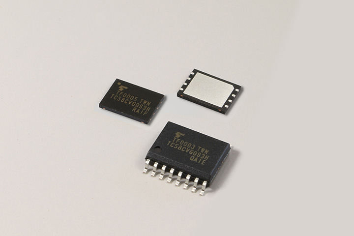
TOKYO — Toshiba Corporation (TOKYO: 6502) today launched a new line-up of NAND flash memory products for embedded applications that are compatible with the widely used Serial Peripheral Interface (SPI). Wide ranging applications for the new “Serial Interface NAND” include such consumer applications as flat-screen TVs, printers and wearable devices, and industrial applications, including robots. Users can choose from a wide line-up of 12 products that offers three densities, 1Gbit, 2Gbit and 4Gbit; two packages, WSON*1 and SOP*2; and two power supply voltages. Samples shipment starts today and mass production is scheduled to begin with the 1Gbit products from December. Mass production of the remaining line-up will follow.
Compatibility with the widely used SPI, which can be controlled with just six pins, allows the new “Serial Interface NAND” to be used as SLC NAND flash memory, with a low pin count, small package and large capacity.
NOR flash memory is typically used in embedded applications for consumer and industrial devices. However, in order to realize extra functionality in embedded devices, demand is growing for larger memory densities for saving software (including boot up programs, firmware, and embedded OS) and data (including log data). This is driving demand for SLC NAND flash memory, which offers higher density and reliability and a lower bit cost than NOR flash memory.
By adding the “Serial Interface NAND” to its product line-up, Toshiba aims to meet wide ranging market needs and to expand the market for NAND flash memory.
*1 WSON: Very-Very thin Small Outline No Lead Package
*2 SOP: Small Outline Package
Outline of the New Products:
* Table can be scrolled horizontally.
| Part Number | Density | I/O | Voltage | Package | Mass Production |
|---|---|---|---|---|---|
| TC58CVG0S3HRAIF | 1Gbit | x1, x2, x4 | 3.3V | WSON |
Dec. 2015 |
TC58CVG0S3HQAIE |
SOP | Dec. 2015 | |||
| TC58CYG0S3HRAIF | 1.8V | WSON | 1Q(Jan.-Mar.) 2016 | ||
| TC58CYG0S3HQAIE | SOP | 1Q(Jan.-Mar.) 2016 | |||
| TC58CVG1S3HRAIF | 2Gbit | 3.3V |
WSON | 1Q(Jan.-Mar.) 2016 | |
| TC58CVG1S3HQAIE | SOP | 1Q(Jan.-Mar.) 2016 | |||
| TC58CYG1S3HRAIF | 1.8V | WSON | 1Q(Jan.-Mar.) 2016 | ||
| TC58CYG1S3HQAIE | SOP | 1Q(Jan.-Mar.) 2016 | |||
| TC58CVG2S0HRAIF | 4Gbit | 3.3V | WSON | Dec. 2015 | |
| TC58CVG2S0HQAIE | SOP | Dec. 2015 | |||
| TC58CYG2S0HRAIF | 1.8V | WSON | 1Q(Jan.-Mar.) 2016 | ||
| TC58CYG2S0HQAIE | SOP | 1Q(Jan.-Mar.) 2016 |
Key Features of the New Products:
- Uses cutting-edge 24nm process technology for SLC NAND.
- Compatible with the widely used SPI, which can be controlled with a low pin count of six pins.
- Available in small and versatile packages. The WSON package is 6.0mm×8.0mm and the SOP package is 10.3mm×7.5mm. BGA*3 packaged products are also under development, with sample shipments scheduled for the first quarter (Jan.-Mar.) of 2016. The packages and the pin assignments are compatible with common serial flash memories.
- Embedded ECC (Error Correction Code) with bit flip count report function.
- Embedded data protection features.
*3 BGA: Ball Grid Array. The package will be 6.0mm×8.0mm, 5 ball×5 ball.
Key Specifications of the New Products:
|
Density |
1Gbit / 2Gbit / 4Gbit |
|---|---|
|
Page Sizes |
2KByte (1Gbit, 2Gbit), 4KByte (4Gbit) |
|
Interface |
Serial Peripheral Interface Mode 0, Mode 3 |
|
I/O |
x1, x2, x4 |
|
Voltages |
2.7-3.6V, 1.7-1.95V |
|
Operating Temperature Range |
-40℃ to 85℃ |
|
Packages |
|
|
Others |
|
Customer Inquiries:
Mobile Memory Sales & Marketing Department
Tel: +81-3-3457-3401